The main difference between a Zener diode and a Schottky diode is that a Zener diode regulates voltage in reverse bias, while a Schottky diode has low forward voltage drop for high-speed switching.
Diodes are essential semiconductor devices used in electronics for various applications. Among them, Zener diodes and Schottky diodes serve distinct purposes. While Zener diodes are designed for voltage regulation, Schottky diodes are known for fast switching and low forward voltage drop. Understanding their differences helps in selecting the right diode for specific applications.
What is Zener Diode?
A Zener diode is a special type of semiconductor device designed to allow current to flow in both forward and reverse bias. Unlike a regular PN junction diode, which blocks current in reverse bias, a Zener diode is built to conduct in reverse when a specific voltage, known as the Zener breakdown voltage, is reached. This unique property makes it highly suitable for voltage regulation and circuit protection applications.
The structure of a Zener diode consists of a heavily doped PN junction, which creates a narrow depletion region. This heavy doping allows the diode to withstand high electric fields, enabling it to enter breakdown mode without damage.
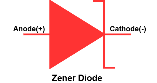
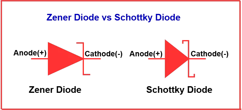
The symbol of a Zener diode is similar to a regular diode but has bent edges at the cathode, representing its ability to conduct in reverse breakdown. The anode is marked with a straight line, while the cathode side has angular bends, visually distinguishing it from a standard diode.
The construction of a Zener diode involves using heavily doped silicon or germanium materials. The doping level is much higher than in a standard PN junction diode, resulting in a lower breakdown voltage. The diode is enclosed in a protective glass or plastic casing to ensure durability and stable performance in electronic circuits. Its design allows it to handle sudden voltage spikes without failure, making it a reliable choice for power regulation.
The working of a Zener diode is based on its ability to regulate voltage. In forward bias, it behaves like a normal diode, allowing current to flow. However, in reverse bias, when the applied voltage exceeds the Zener breakdown voltage, it starts conducting in reverse without damage. This property makes it ideal for voltage regulation and overvoltage protection, ensuring that circuits operate within safe voltage limits.
Key characteristics of a Zener diode include its breakdown voltage, power dissipation capacity, temperature stability, and dynamic resistance. The breakdown voltage is carefully controlled during manufacturing, making it highly precise for use in regulated power supplies and overvoltage protection circuits.
The important parameters of a Zener diode include Zener voltage (Vz), Zener impedance (Zz), reverse current (Iz), and power rating. The Zener voltage determines the point at which the diode starts conducting in reverse, while the power rating defines how much current it can handle safely.
The Zener breakdown occurs due to two primary mechanisms: avalanche breakdown and Zener breakdown. Avalanche breakdown happens in diodes with a higher breakdown voltage (above 5V), where electrons gain enough energy to knock off more electrons, creating a chain reaction. Zener breakdown, on the other hand, occurs in diodes with a low breakdown voltage (below 5V), where a strong electric field breaks covalent bonds, generating charge carriers.
Due to these properties, Zener diodes are widely used in voltage regulators, surge protectors, and circuit protection applications. Their ability to maintain a stable voltage makes them an essential component in power supply designs, ensuring reliable operation of electronic devices. The combination of precise breakdown voltage, durability, and efficiency makes them a preferred choice in power electronics and voltage stabilization circuits.
What is Schottky Diode?
A Schottky diode is a special type of semiconductor diode designed for high-speed switching and low forward voltage drop. Unlike a conventional PN junction diode, which consists of a p-type and n-type semiconductor, a Schottky diode forms a metal-semiconductor junction. This unique construction reduces power losses, making it ideal for high-frequency applications.
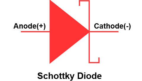
The symbol of a Schottky diode is similar to a regular PN junction diode, but it has an additional curve on the cathode side, representing the metal-semiconductor junction. This symbol differentiates it from standard diodes and highlights its special electrical properties.
The structure of a Schottky diode consists of a metal and an n-type semiconductor junction, eliminating the need for a depletion region like in a standard diode. The metal used is typically gold, platinum, chromium, or tungsten, while the semiconductor is usually n-type silicon. This metal-semiconductor contact leads to fast operation and low resistance.
The construction of a Schottky diode involves depositing a metal layer onto a lightly doped n-type semiconductor. Unlike traditional diodes that require two doped semiconductor regions, the Schottky diode relies on the metal’s work function to create a barrier for current flow. This design results in minimal charge storage, enhancing its switching speed.
The working of a Schottky diode is based on the movement of electrons across the metal-semiconductor junction. When forward biased, electrons from the n-type region move into the metal, allowing current flow with very low voltage drop (typically 0.2V to 0.4V). In reverse bias, the barrier prevents current, blocking conduction.
Key characteristics of a Schottky diode include low forward voltage drop, high-speed switching, minimal charge storage, and high efficiency. Due to its low voltage drop, it reduces power dissipation, improving energy efficiency in circuits. Its fast recovery time makes it highly suitable for RF and digital applications.
The important parameters of a Schottky diode include forward voltage drop (Vf), reverse leakage current (Ir), maximum current rating (If), and breakdown voltage (Vbr). The low forward voltage drop leads to lower heat generation, while higher reverse leakage is a trade-off due to the absence of a depletion layer.
A Schottky diode is a perfect fit for switching applications due to its ultra-fast response time. Since it does not have a charge storage issue like PN junction diodes, it can switch on and off almost instantly. This property makes it ideal for power rectifiers, RF circuits, and digital logic applications.
The advantages of a Schottky diode include lower power loss, high efficiency, fast switching speed, and reduced heat generation. It is widely used in solar cells, power management circuits, and high-frequency applications where efficiency is crucial. However, it has some drawbacks as well.
The disadvantages of a Schottky diode include higher reverse leakage current, lower breakdown voltage, and sensitivity to temperature variations. Due to its low breakdown voltage, it is not suitable for high-voltage applications, and its higher leakage current can cause issues in low-power circuits.
Difference between Zener Diode and Schottky Diode
The table below highlights the key differences between Zener diodes and Schottky diodes in terms of their structure, characteristics, and applications.
| Parameter | Zener Diode | Schottky Diode |
|---|---|---|
| Definition | A diode designed to operate in reverse breakdown to regulate voltage. | A diode with a metal-semiconductor junction for fast switching. |
| Construction | Made of heavily doped p-n junction. | Made with a metal and n-type semiconductor junction. |
| Functionality | Used for voltage regulation by maintaining a stable voltage. | Used for high-speed switching and low power loss. |
| Forward Voltage Drop | Around 0.7V (Silicon) and 0.3V (Germanium). | Very low, typically 0.2V to 0.4V. |
| Reverse Breakdown Voltage | Operates in reverse bias breakdown region. | Has a lower breakdown voltage compared to Zener diodes. |
| Switching Speed | Slower compared to Schottky diodes. | Extremely fast switching response. |
| Reverse Leakage Current | Low leakage current. | Higher leakage current compared to Zener diodes. |
| Efficiency | Used to stabilize voltage, not for efficiency. | Highly efficient due to low power loss. |
| Applications | Used in voltage regulation, surge protection, and reference circuits. | Used in RF circuits, rectifiers, and digital circuits. |
| Symbol | Similar to a PN junction diode with bent edges indicating breakdown region. | Similar to a PN junction diode with a curved cathode line. |
| Current Flow Direction | Conducts only in reverse breakdown mode. | Conducts in forward bias and blocks in reverse bias. |
| Power Dissipation | Higher due to reverse breakdown operation. | Lower due to minimal forward voltage drop. |
| Temperature Sensitivity | Less affected by temperature variations. | More sensitive to temperature changes. |
| Use in Clamping Circuits | Not suitable for high-speed clamping. | Ideal for fast clamping in digital circuits. |
| Cost | Generally cheaper due to simple manufacturing. | More expensive due to metal-semiconductor junction. |
This table provides a detailed comparison of Zener and Schottky diodes, highlighting their differences in functionality, efficiency, and applications.
Conclusion
In conclusion, Zener diodes and Schottky diodes serve distinct purposes in electronic circuits due to their structural and functional differences. Zener diodes are designed to operate in the reverse breakdown region, making them ideal for voltage regulation and surge protection. In contrast, Schottky diodes have a low forward voltage drop and fast switching speed, making them suitable for high-frequency and power-efficient applications.
While Zener diodes provide stable voltage references, Schottky diodes are preferred for rectification and clamping circuits due to their low power loss. Choosing the right diode depends on the specific requirements of a circuit, such as efficiency, response time, and voltage stability. Understanding these differences helps in selecting the best diode for optimal circuit performance.
Read Next: