The key difference between a PN junction diode and a Zener diode lies in their current flow behavior. A PN junction diode permits current flow only in the forward direction, blocking it in reverse. In contrast, a Zener diode allows current to flow in both forward and reverse directions, making it ideal for voltage regulation applications.
Before exploring the differences between a PN junction diode and a Zener diode, it is important to first understand what each of these diodes is. Both are semiconductor devices that serve vital roles in electronics, but they function differently based on their design and purpose. Let’s understand these.
What is PN Junction Diode?
A PN junction diode is a semiconductor device that allows current to flow in only one direction. It consists of two terminals: the anode (P-side) and the cathode (N-side). The P-side has excess holes (positive charge carriers), while the N-side has excess electrons (negative charge carriers). This junction forms the basis of rectification in electronic circuits.
The construction of a PN junction diode involves doping a semiconductor material, typically silicon or germanium, to create two distinct regions: the P-type (positive) and N-type (negative). These are joined together to form the junction. A depletion region is created at the junction due to electron-hole recombination, which acts as an insulator in the absence of an external voltage.
The working principle of a PN junction diode depends on the applied voltage. In forward bias, when the anode is connected to the positive terminal of a battery and the cathode to the negative, the depletion region narrows, allowing current to flow. In reverse bias, the depletion region widens, blocking current flow. But why does a diode block reverse current? This is due to the potential barrier formed at the junction.
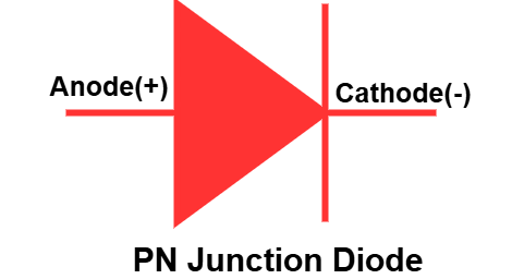
The symbol of a PN junction diode consists of a triangle pointing towards a vertical line. The triangle represents the P-side (anode), and the line represents the N-side (cathode). This symbol visually indicates the direction of allowed current flow, making circuit analysis easier. But how do you identify anode and cathode? The longer lead in a diode usually represents the anode.
The advantages of a PN junction diode include its simple design, low cost, fast switching speed, and high efficiency in rectification. It is widely used in power supplies, clippers, clampers, and voltage rectifiers. However, does it work in all conditions? No, it has limitations in high voltage and high-frequency applications.
The disadvantages of a PN junction diode include reverse breakdown at high voltage, temperature sensitivity, and limited power handling capability. Can it be used as a voltage regulator? No, for voltage regulation, a Zener diode is preferred, as it operates in reverse bias without damage.
In conclusion, a PN junction diode is a fundamental electronic component used for rectification and signal processing. Understanding its working, advantages, and limitations helps in selecting the right diode for a specific application, ensuring efficient circuit performance.
What is Zener Diode?
A Zener diode is a specially designed semiconductor device that allows current to flow in both forward and reverse directions. It has two terminals: the anode (P-side) and the cathode (N-side). Unlike a regular diode, it is designed to operate in reverse breakdown mode without getting damaged, making it ideal for voltage regulation.
The construction of a Zener diode is similar to a PN junction diode, but it is heavily doped to create a thin depletion region. This heavy doping allows the diode to undergo a controlled breakdown at a precise voltage, known as the Zener voltage. It is available in different voltage ratings, making it versatile for different circuit applications.
The working principle of a Zener diode depends on the applied voltage. In forward bias, it behaves like a normal diode, allowing current to flow. In reverse bias, it blocks current until the applied voltage reaches the Zener breakdown voltage, at which point it starts conducting in reverse. But why doesn’t it get damaged? It is designed to withstand breakdown conditions without failure.
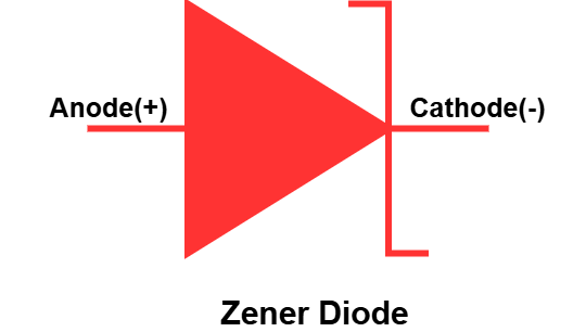
The symbol of a Zener diode is similar to a PN junction diode but with bent edges on the cathode side. This differentiates it from a regular diode and indicates its ability to function in reverse breakdown mode. How can you identify a Zener diode in a circuit? It is usually connected in reverse bias for voltage regulation purposes.
The advantages of a Zener diode include precise voltage regulation, small size, low cost, and high reliability. It is widely used in power supplies, voltage reference circuits, and surge protection. Can it handle large currents? No, Zener diodes are designed for low-power applications and require a current-limiting resistor to avoid excessive heat.
The disadvantages of a Zener diode include limited current handling capacity, power dissipation, and voltage variation with temperature. Is a Zener diode better than a voltage regulator IC? While integrated voltage regulators are more efficient for high-power applications, Zener diodes are simpler and cheaper for low-power voltage stabilization.
A Zener diode is a perfect fit for a voltage regulator because it maintains a constant output voltage even when the input voltage or load resistance varies. This makes it highly effective in stabilizing circuits, preventing voltage fluctuations, and protecting sensitive electronic components from damage, ensuring smooth and reliable performance.
Now that we have a basic understanding of PN junction diode and zener diode, we can explore their key differences and how they are used in various applications.
Difference Between PN Junction Diode and Zener Diode
A PN junction diode and a Zener diode are both semiconductor devices but have different functionalities. The PN junction diode allows current flow in only one direction, while the Zener diode permits current flow in both forward and reverse directions under breakdown conditions. The table below highlights the key differences between them.
| Parameter | PN Junction Diode | Zener Diode |
|---|---|---|
| Definition | A two-terminal semiconductor device formed by joining a P-type and N-type semiconductor. | A special type of diode optimized to operate in reverse breakdown mode. |
| Doping Level | The doping level of P-type and N-type semiconductors is low. | The P-type and N-type regions are highly doped to achieve controlled breakdown. |
| Width of Depletion Layer | The depletion layer is wider due to low doping. | The depletion layer is narrow due to high doping. |
| Effect of Reverse Current | High reverse current can permanently damage the diode. | Designed to withstand reverse current without damage. |
| Breakdown Voltage | Has a higher breakdown voltage, usually in the hundreds of volts. | Has a lower breakdown voltage, typically between 2V to 200V. |
| Biasing Condition | Operates only in forward bias, meaning current flows from anode to cathode. | Operates in both forward and reverse bias due to Zener breakdown. |
| Ohm’s Law | Obeys Ohm’s law in forward bias conditions. | Does not obey Ohm’s law in the breakdown region. |
| Manufacturing Materials | Typically made from silicon or germanium (silicon being more common). | Material is chosen based on the desired breakdown voltage. |
| Current Flow | Unidirectional (allows current only in one direction). | Bidirectional (allows current in forward and reverse directions under breakdown). |
| Behavior in Biasing | Acts as a closed switch in forward bias and an open switch in reverse bias. | Acts as a normal diode in forward bias and conducts in reverse bias during breakdown. |
| Application | Commonly used for rectification, clamping, and clipping circuits. | Mainly used as a voltage regulator and protection circuit. |
| Power Dissipation | Generates less heat due to low reverse current. | May dissipate more power in reverse bias, requiring a series resistor for protection. |
| Temperature Sensitivity | Less sensitive to temperature variations. | More sensitive, and breakdown voltage varies with temperature. |
| Response Time | Has a faster switching speed, making it suitable for high-frequency applications. | Slower response due to the breakdown process in reverse bias. |
| Symbol | Represented by a triangle pointing toward a vertical line (standard diode symbol). | Similar to a PN junction diode, but with bent edges at the cathode side. |
| Cost | Less expensive due to simpler design. | Slightly costlier due to specialized breakdown characteristics. |
Conclusion
The PN junction diode and Zener diode serve different purposes in electronic circuits due to their unique characteristics. A PN junction diode is primarily used for rectification and signal processing, allowing current to flow in only one direction and blocking reverse current. In contrast, a Zener diode is specifically designed to operate in reverse breakdown mode, making it ideal for voltage regulation and protection circuits.
The key differences lie in their doping levels, depletion layer width, breakdown voltage, and response to reverse bias conditions. While a PN junction diode gets damaged under high reverse voltage, a Zener diode is built to withstand and regulate voltage effectively.
In summary, if the goal is rectification, a PN junction diode is the best choice. However, for voltage stabilization and overvoltage protection, the Zener diode is the preferred option. Their distinct functionalities make them essential components in different areas of electronics and power management.
Read Next: