Discover the key differences between NPN and PNP transistors, including their structure, working principle, current flow, and applications. Learn why NPN transistors are preferred in most circuits.
PNP and NPN transistors are types of Bipolar Junction Transistors (BJTs). They are essential components in electrical and electronic circuits. These transistors work using holes and electrons. They function as amplifiers, switches, and oscillators.
In a PNP transistor, holes are the majority charge carriers, while in an NPN transistor, electrons are the majority charge carriers. However, Field Effect Transistors (FETs) use only one type of charge carrier.
The main difference between NPN and PNP transistors is how they receive power. An NPN transistor turns ON when current flows through its base terminal. In an NPN transistor, current flows from the collector to the emitter.
A PNP transistor turns ON when there is no current at the base terminal. In a PNP transistor, current flows from the emitter to the collector. This means a PNP transistor switches ON with a low signal, while an NPN transistor switches ON with a high signal.
What is a PNP Transistor?
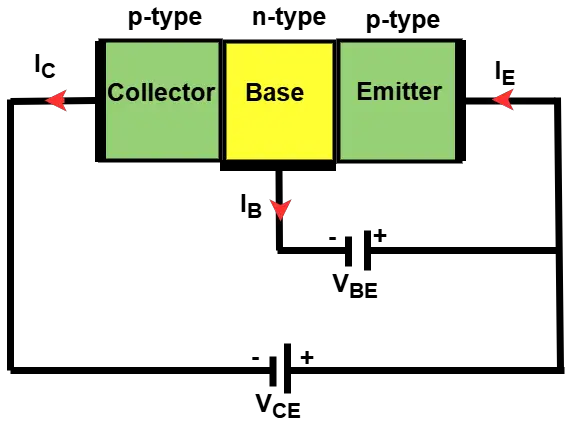
PNP stands for Positive-Negative-Positive and is also known as a sourcing transistor. It is a type of Bipolar Junction Transistor (BJT) where the majority charge carriers are holes.
In a PNP transistor:
- The ‘P’ in the name indicates the positive polarity required at the emitter terminal.
- The ‘N’ represents the negative polarity needed at the base terminal.
This transistor operates similarly to an NPN transistor, but the materials used for the emitter (E), base (B), and collector (C) are different.
The base-collector (BC) junction is always reverse-biased, meaning a negative voltage must be applied to the collector terminal. As a result:
- The base terminal must be negative relative to the emitter terminal.
- The collector terminal must be more negative than the base terminal.
A PNP transistor works by controlling the flow of current through its terminals. When a small current flows from the emitter to the base, it allows a larger current to flow from the emitter to the collector. This makes PNP transistors useful in switching and amplification applications. Unlike an NPN transistor, which turns ON with a positive base current, a PNP transistor turns ON when the base is at a lower voltage than the emitter.
In circuit applications, PNP transistors are often used in high-side switching configurations. They are ideal for controlling loads that need to be connected to the positive supply voltage. When the base voltage is low, the transistor allows current to pass from the emitter to the collector, turning the circuit ON. When the base voltage is high, the transistor turns OFF, stopping the current flow.
PNP transistors are widely used in analog circuits, push-pull amplifier stages, and motor driver circuits. They are often paired with NPN transistors in complementary circuits, such as in H-bridge motor controllers and class B amplifiers. Due to their switching characteristics, PNP transistors play a crucial role in electronic systems that require efficient power control.
Construction of PNP Transistor
The construction of a PNP transistor is similar to that of an NPN transistor, except that the biasing of current and voltage directions is reversed. A PNP transistor can be used in three configurations: common base, common emitter, and common collector.
In a PNP transistor:
- The voltage between the base (B) and emitter (E) (VBE) is negative at the base terminal and positive at the emitter terminal.
- The base terminal is always biased negatively with respect to the emitter terminal.
- The voltage VBE is positive when compared to the collector-emitter voltage (VCE).
The circuit connections of a PNP transistor are as follows:
- The emitter terminal is connected to Vcc through a load resistor (RL). This resistor limits the current flowing through the transistor to protect it from excessive current.
- The base terminal (VB) is connected to a base resistor (RB), which is biased negatively with respect to the emitter terminal.
To allow base current to flow in a PNP transistor, the base terminal must be more negative than the emitter terminal by approximately 0.7V for a silicon transistor or lower for other materials.
The key difference between PNP and NPN transistors lies in their biasing and current flow. In a PNP transistor, the current and voltage polarities are always opposite to those in an NPN transistor.
What is an NPN Transistor?
The term NPN stands for Negative-Positive-Negative and is also known as a sinking transistor. An NPN transistor is a type of Bipolar Junction Transistor (BJT) where the first ‘N’ represents a negatively charged layer, the ‘P’ represents a positively charged layer, and the final ‘N’ represents another negatively charged layer. The positive (P) layer is positioned between the two negative (N) layers.
NPN transistors are widely used in electronic circuits for switching applications and signal amplification. When an electrical signal is applied to the base terminal, it controls the flow of current between the collector and emitter terminals. This allows the transistor to amplify weak signals or act as an electronic switch.
An NPN transistor has three terminals:
- Base (B) – Receives the input signal.
- Collector (C) – Collects the main current flow.
- Emitter (E) – Passes the amplified or switched current into the circuit.
When the base terminal receives a small positive voltage, it allows a larger current to flow from the collector to the emitter. This is the opposite of how a PNP transistor works, where current flows from the emitter to the collector.
NPN transistors are widely used because they are easy to manufacture and efficient in performance. They are made from semiconductor materials like silicon, which has controlled conductivity—allowing some current to pass through but not as much as metals. Silicon-based NPN transistors are the most commonly used in modern electronic circuits due to their reliability, cost-effectiveness, and ease of integration into various applications.
NPN transistors play a crucial role in computer circuit boards, where they help process binary information. These transistors act as tiny switches that turn ON and OFF, representing binary code (1s and 0s). When a strong electrical signal is present, the transistor turns ON. When no signal is present, it turns OFF. This rapid switching ability enables computers and digital devices to process information efficiently.
Construction of an NPN Transistor
The NPN transistor consists of three terminals: Base (B), Collector (C), and Emitter (E). The base terminal always remains positive (+Ve) concerning the emitter terminal, which is negative (-Ve). Similarly, the collector terminal is also positive (+Ve) concerning the emitter terminal.
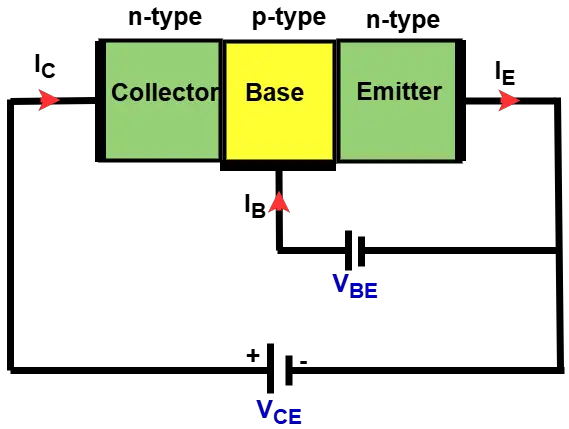
In this transistor, the collector terminal is connected to the VCC power supply through a load resistor (RL). This resistor limits the current flow, ensuring that excessive current does not pass through the base terminal. The flow of electrons through the base controls the transistor’s operation. The key function of the NPN transistor is its ability to amplify signals, which happens due to the interaction between the input (base) and output (collector-emitter) circuits.
An NPN transistor is a current-controlled device. When it is turned ON, a large collector current (IC) flows from the collector to the emitter. However, this happens only when a small base current (IB) is applied. The transistor is called bipolar because it operates based on the interaction of two types of charge carriers: electrons and holes.
The ratio of collector current (IC) to base current (IB) is called the DC current gain (β or hFE). This value determines how much the transistor amplifies the input current. For standard transistors, β (hFE) can be as high as 200.
When an NPN transistor operates in the active region, the base current (IB) acts as the input, while the collector current (IC) is the output. Another important parameter is alpha (α), which is the ratio of collector current (IC) to emitter current (IE).
Since the emitter current (IE) is the sum of the base current (IB) and collector current (IC), the alpha (α) value is very close to 1. For most low-power signal transistors, α ranges between 0.950 and 0.999. This high efficiency makes NPN transistors ideal for amplification and switching applications in electronic circuits.
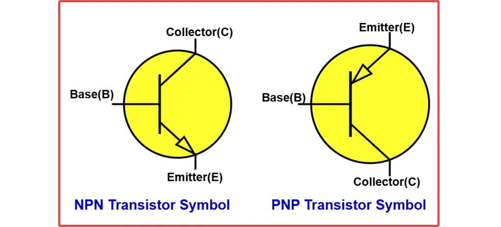
Transistor Symbols
The symbols of NPN and PNP transistors are very similar, with the main difference being the direction of the arrow at the emitter terminal.
- In an NPN transistor, the arrow points outward, indicating that current flows from the emitter to the circuit.
- In a PNP transistor, the arrow points inward, showing that current flows from the emitter to the collector.
The PNP transistor symbol shows that current moves from the emitter to the collector, while in an NPN transistor, the current flows from the collector to the emitter. This difference helps identify how each transistor operates in a circuit.
Which is Better: NPN or PNP?
Both NPN and PNP transistors are BJTs (Bipolar Junction Transistors) used for switching and amplification. However, NPN transistors are generally preferred in most applications.
The main reason is that NPN transistors use electrons as charge carriers, while PNP transistors use holes. Electrons move faster than holes, making NPN transistors more efficient for high-speed switching and signal amplification.
Another key difference is how voltage is applied to the base, emitter, and collector terminals. Since electrons move more easily than holes, NPN transistors offer better conductivity and faster response times. That’s why NPN transistors are more commonly used in circuits than PNP transistors. However, both types are essential and are chosen based on the specific circuit requirements.
Difference Between NPN and PNP Transistor
The main difference between NPN and PNP transistors is the direction of current flow and the type of charge carriers responsible for conduction.
- In an NPN transistor, current flows from the collector to the emitter when a positive voltage is applied to the base.
- In a PNP transistor, current flows from the emitter to the collector when a negative voltage is applied to the base.
The following table summarizes the key differences between NPN and PNP transistors:
| Feature | NPN Transistor | PNP Transistor |
|---|---|---|
| Structure | P-layer separates two N-type layers | N-layer separates two P-type layers |
| Full Form | Negative-Positive-Negative | Positive-Negative-Positive |
| Current Flow | From collector to emitter | From emitter to collector |
| Charge Carriers | Electrons (majority), Holes (minority) | Holes (majority), Electrons (minority) |
| Activation | Turns ON when electrons enter the base | Turns ON when holes enter the base |
| Internal Current Flow | Developed due to electron movement | Developed due to hole movement |
| External Current Flow | Due to holes | Due to electrons |
| Ground Signal | Low | High |
| Base Current Flow | From emitter to base | From base to emitter |
| Collector-Base Junction | Reverse biased | Reverse biased |
| Emitter-Base Junction | Forward biased | Forward biased |
| Collector Terminal | Connected to positive voltage | Connected to negative voltage |
| Switching Speed | Faster | Slower |
| Turning Off Condition | Stops working when base current decreases | Stops working when base current is present |
Since electrons move faster than holes, NPN transistors have higher speed and efficiency, making them the preferred choice for most applications. However, PNP transistors are still used in specific circuits where their characteristics are needed.
Key Differences Between NPN and PNP Transistors
NPN and PNP transistors are three-terminal semiconductor devices used for switching and amplification. Each bipolar junction transistor (BJT) consists of two PN junctions, forming a sandwich-like structure.
There are only two possible bipolar sandwich structures:
- NPN transistor (P-layer between two N-layers)
- PNP transistor (N-layer between two P-layers)
The NPN transistor is more commonly used because it has higher electron mobility, allowing it to carry more current and operate faster. It is also easier to manufacture using silicon.
Main Differences Between NPN and PNP Transistors
- Structure:
- NPN transistor: Has a P-layer sandwiched between two N-layers.
- PNP transistor: Has an N-layer sandwiched between two P-layers.
- Current Flow:
- NPN transistor: Current flows from collector to emitter.
- PNP transistor: Current flows from emitter to collector.
- Voltage Application:
- NPN transistor: A positive voltage is applied to the collector terminal to allow current flow.
- PNP transistor: A positive voltage is applied to the emitter terminal to allow current flow.
- Working Principle:
- NPN Transistor:
- When the base current increases, the transistor switches ON, allowing current to flow from collector to emitter.
- When the base current decreases, the transistor switches OFF, stopping the current flow.
- PNP Transistor:
- When current is present at the base, the transistor turns OFF.
- When there is no base current, the transistor switches ON.
- NPN Transistor:
Conclusion
- NPN transistors are preferred in most applications because they operate faster and handle higher currents due to better electron mobility.
- PNP transistors are used in specific circuits, especially in complementary designs with NPN transistors.
Read Next: