A photodiode is a semiconductor diode made of silicon, germanium, or compound semiconductor. It converts light energy into electrical current in reverse bias, and not in the forward bias. Unlike other diodes, it is containing a p-n junction and is designed to operate in the reverse bias before the breakdown voltage.
Photodiodes are also known by other names, such as
- Photo-detector
- Photo-sensor
- Light detector
Construction of Photodiode

It is equipped with two metal wires and is mounted in a plastic or metal housing with a transparent window. The photodiode is constructed in such a way that it is fully exposed to light through its transparent body.
When light strikes the junction, a current or voltage develops. A light detector may have a larger area to enhance photo response. It is capable of detecting radiation from the optical domain and transforming it into an electrical signal.
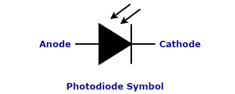
In electrical diagrams, as shown in the above figure, a photodiode is referred to as a diode with three arrows pointing toward it. The three arrows symbolize the incident radiation on the photodiode. It is not to be confused with the designation of the LED whose arrows point away.
Modern electronic devices use them extensively.

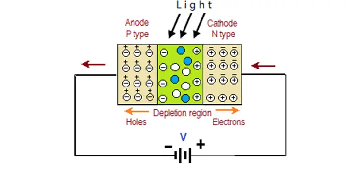
The creation of electron-hole pairs in the depletion region can be seen in the above figure. A reverse-biased photodiode produces a current proportional to the light intensity. The depletion region is comprised the blue-filled circles and white circles. Blue circles represent electrons and the holes are white circles. These are semiconductor diodes in which the amount of reverse current depends on the illumination.
Infra-Red (IR) sensitive devices use indium antimonide (InSb), indium-gallium arsenide (InGaAs), germanium (Ge), or cadmium-mercury telluride (HgCdTe).
UV-sensitive devices typically use silicon carbide (SiC).
Silicon (Si) photodiodes are sensitive to visible light.
Various materials can be used to make photodiodes. The commonly used materials are silicon (Si), germanium (Ge), indium gallium arsenide (InGaAs), and Indium antimonide (InSb). The choice of the semiconductor material is determined by the properties such as sensitivity, cut-off frequency, dark current, etc.
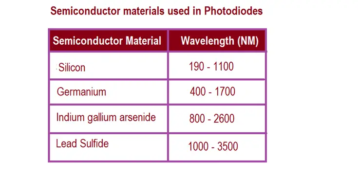
The photodiodes must desire wavelength range to perform these requirements. They are suitable for the wavelength ranges given in the table below.

Photodiode Symbol
The symbol of the photodiode is the same as that of a normal p-n junction diode, except it has arrows striking the diode. The arrows striking the diode show light or photons.

Modes of Operation of Photodiode
It depends on the mode of the operation (forward or reverse bias). Based on the biasing applied to them, the diodes can be operated in one of three modes.
1. Photovoltaic mode
2. Photoconductive mode
3. Avalanche diode mode
1. Photovoltaic Mode
If the photodiode is not biased, it restricts the flow of current out of the device. Hence, there is a voltage buildup. In this case, it behaves like a solar cell. When it is forward-biased, a “dark current” begins to flow across the p-n junction in the opposite direction to the photocurrent. A dark current is a current that exists even when the diode is not exposed to light. These diodes are useful in light intensities that are generally below 350 KHz (Kilohertz) and applications involving low frequencies. There is a low output voltage, usually, the photodiode output requires an amplifier in many instances.
2. Photoconductive Mode
A reverse bias is applied across the photodiode in the photoconductive mode. The applied reverse bias generates a depletion region at the P-N junction. The greater the polarization, the wider the depletion zone. As with the widened depletion region, the capacitance at the junction is reduced. Thereby resulting in faster response, and exhibiting low noise.
3. Avalanche Diode Mode
They have a similar structure to any other photodiode; avalanche mode operates the photodiode in a high reverse bias state. As the reverse bias is further increased, the photodiode operates as an avalanche diode. This allows the multiplication of each photon-produced electron-hole pair due to avalanche breakdown. This results in an internal gain and increased sensitivity. This resembles, in its operation, a photomultiplier tube.
Photodiode Working
In general, a photodiode is a p-n junction open to light. Under the influence of light in the p-n junction area, charge carriers (electrons and holes) are generated. They pass through the junction and cause a voltage across the photodiode or current flow in a closed circuit.
Holes move to the p-zone and electrons accumulate in the n-zone. Electrons charge the n-zone negatively, and holes charge the p-zone positively. The potential difference is formed. Higher the illuminance, the greater the reverse current.
If the semiconductor is in the dark, its properties are similar to those of a conventional diode. In the absence of illumination, the results will be similar to testing a conventional diode.
The photodiode, depending on its material, is designed to record the luminous flux in the infrared, optical, and ultraviolet wavelength range. Photodiodes are made from silicon, germanium, gallium arsenide, gallium indium arsenide, and other materials.
In photovoltaic mode, the photodiode operates without an external power supply. In this mode, it can work as a sensor or as a power element (solar battery), since under the influence of light a voltage appears across the photodiode.
V-I Characteristics of Photodiode
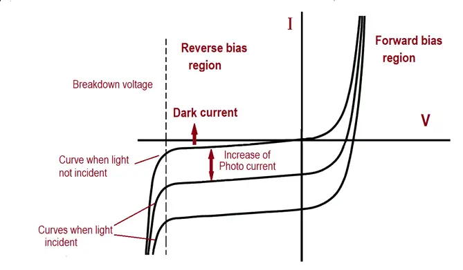
To better understand the working modes of the photodiode, one needs to consider its voltage-current characteristics. The chart consists of 4 areas, called quadrants. Photodiode mode corresponds to the work in the 3rd quadrant.

In the absence of radiation, the graph is the inverse branch of the voltage-current characteristic of a conventional semiconductor diode. A small reverse current is present, call the dark current (thermal current) of the reverse biased p-n junction.
In the presence of luminous flux, the resistance of the diode decreases, and the reverse current increases. The more light is incident, the more reverse current passes through it. The dependence of the reverse current of the photodiode on the luminous flux in this mode is linear.
The graph shows that the reverse current of the photodiode is weakly dependent on the reverse voltage. By looking at the slope of the graph from zero voltage to breakdown voltage, it is small.
Types of Photodiodes
Based on construction and functions, they are classified into four types.
1. PN Photodiode
2. PIN Photodiode
3. Schottky Photodiode
4. Avalanche Photodiode
1. PN Photodiode
This is the basic form of photodiode and used widely before the development of other diodes. Its size is small than any other photodiode, sensitivity is poor. Also, performance parameters are not better compared to other types of photodiodes.
2. PIN Photodiode
Like any diode in electronics, it consists of a PN junction. The basic configuration was improved by the introduction of the intrinsic zone (I) to perform the P-I-N photodiode.
The large intrinsic zone (I) between the P and N regions makes it possible to fall huge light on it. The increase of a large intrinsic zone makes to increase the gap between P and N areas, thereby resulting in lower capacitance. Hence it efficiently collects light photons better than PN photodiodes.
The PIN photodiode is widely used photodiode.
3. Avalanche photodiode
It works with high reverse voltages. An Avalanche zone allows photogenerated charge carriers to be multiplied. Thereby resulting in very high gain levels but coming with high noise levels. This species is very sensitive. Its function is to convert the luminous flux into an electrical signal, amplified by the avalanche multiplier effect. It can be used in low light output conditions.
Avalanche photodiode (APD) uses a concept called superlattice used in long-wavelength semiconductor materials. Thereby reducing signal transmission noise.
4. Schottky Barrier Photodiode
It offers small diode capacitance as well as super high-speed capability. There is an electric field around the junction of metal and semiconductors. The main difference with conventional P-I-N type photodiodes is the use of basic and not additional charge carriers.
Important Characteristics of Photodiodes
- Speed /Bandwidth
- Dark current
- Maximum allowed photocurrent
- Responsiveness
- Active area
Advantages
- Simple construction
- Inexpensive
- The robust structure has made them popular and successful.
- Faster response, high sensitivity
- Long lifetime
- Low noise.
Disadvantages
- With the increase of the light receiving area, its response time decreases.
- In photovoltaic mode, there is no dark current, but the speed of the collectors will be lower.
Photodiodes Applications
- They are widely used in control systems, metrology, robotics, and other fields.
- They are also used in other components, for example optocouplers, and opto-relays.
- Microcontrollers use these types of diodes in various sensors – end sensors, light sensors, distance sensors, pulse sensors, etc.,
- Optoelectronics integrated circuits – Semiconductors provide optical communication, which ensures effective galvanic isolation of power and control circuits while maintaining functional communication.
- Multi-element photodetectors – Photosensitive devices, photodiodes arrays. An optoelectrical element can perceive not only the characteristic brightness of an object and its change over time but also create a complete visual image.
- Other areas of use – Optic fiber lines (OFC), laser range finders, and positron emission tomography installations.
Comprehensive information, I find the article a catalyst to go through electricvolt.com.
Semiconductor material and it’s wavelength ranges,V-I Characteristics, three modes of operation of laser diodes is interesting to read.Thank you.